
Lab 7 - ECE 421L
October 20, 2021
Prelab Content
Prior to this lab session, we were tasked with backing up our previous work (as usual) as well as finishing Tutorial 5, in which we learned how to design, layout, and simulate a CMOS NAND gate. We were also tasked with giving the entire lab document a quick read through in preparation of the actual lab.
Tutorial 5 Screenshots:

![]()
Postlab Report


8-bit Inverter Simulation Schematic and Results:


As can be observed above in the last image, the inverter gate is functioning properly as it alternates between logic high and logic low as the pulse source oscillates.
Secondly, I performed the same steps but for the AND gate.
Base 1-bit AND Schematic and Symbol:


8-bit AND Schematic and Symbol:


8-bit AND Simulation Schematic and Results:


As can be observed above in the last image, the AND gate is functioning properly as the output only switches to logic high when both inputs are high.
Next, I performed the same steps but for the NAND gate.


8-bit NAND Schematic and Symbol:


8-bit NAND Simulation Schematic and Results:


As can be observed above in the last image, the NAND gate is functioning properly as the output switches to logic high as long as neither or only one of the inputs is logic high.
Next, I performed the same steps but for the OR gate.
Base 1-bit OR Schematic and Symbol:


8-bit OR Schematic and Symbol:


8-bit OR Simulation Schematic and Results:


As can be observed above in the last image, the OR gate is functioning properly as the output is logic high when either or both of the inputs are logic high.
Next, I performed the same steps but for the NOR gate.
Base 1-bit NOR Schematic and Symbol:


8-bit NOR Schematic and Symbol:


8-bit NOR Simulation Schematic and Results:


As can be observed above in the last image, the NOR gate is functioning properly as the output is logic high only when both inputs are logic low.
With that, the all of the gates have now been properly implemented and verified through simulated testing.
The next portion of the lab consisted of examining the provided schematic and symbol on the lab document for a 2-to-1 MUX.
This circuit takes in 2 inputs of data (A and B) as well as a select
input (S which is also inverted to provide Si). The output is assigned
based on the following function: Z = A*S + B*Si.
Essentially, the
value of the select will choose whether A or B is read out to the
console. The data stored in A is output if S is logic high and the data
stored in B is output if S is logic low (because then Si will be logic
high).
We were tasked with implementing this ourselves in Cadence and running simulations to verify it's operation. Additionally, we needed to then create an 8-bit wide word 2-to-1 MUX schematic and symbol along with another simulation.
2-to-1 MUX Schematic:

2-to-1 MUX Symbol:

2-to-1 MUX Simulation Schematic:

2-to-1 MUX Simulation Results:

As can be observed above in the last image, the 2-to-1 MUX is functioning properly as the output is aligned to the provided equation Z = A*S + B*Si.
Now, here are the documentation images for the implementation of the 8-bit wide word 2-to-1 MUX.
8-bit 2-to-1 MUX Schematic:

8-bit 2-to-1 MUX Symbol:

8-bit 2-to-1 MUX Simulation Schematic:

8-bit 2-to-1 MUX Simulation Results:

As can be observed above in the last image, similar to the 1-bit 2-to-1 MUX, the 8-bit wide word 2-to-1 MUX is functioning properly as the output is aligned to the provided equation Z = A*S + B*Si. Note that as the 8-bit MUX schematic has the inverter built-in for grabbing Si from S, Si is not shown on the simulation results; however, the value of Si at any point can be extrapolated simply by taking the inverse of S (Sin in the plot).
For the last portion of the lab, we drafted a schematic/symbol of the full-adder seen in Fig. 12.20 using 6u/0.6u devices (both PMOS and NMOS). Then, used this newly created symbol to draft an 8-bit adder schematic/symbol.
Full-Adder Schematic:

Full-Adder Symbol:

Full-Adder Layout:

Full-Adder DRC Clean:

Full-Adder Extracted Layout:


Full-Adder LVS Clean:

Now that all the necesarry drafting was done for the base Full-Adder, it was now time to transition to drafting the 8-bit Full-Adder. This process was more or less the same as implementing the 8-bit versions of all of the prior gates in this lab.


8-bit Full-Adder Layout (Zoom Fit):


8-bit Full-Adder DRC Clean:

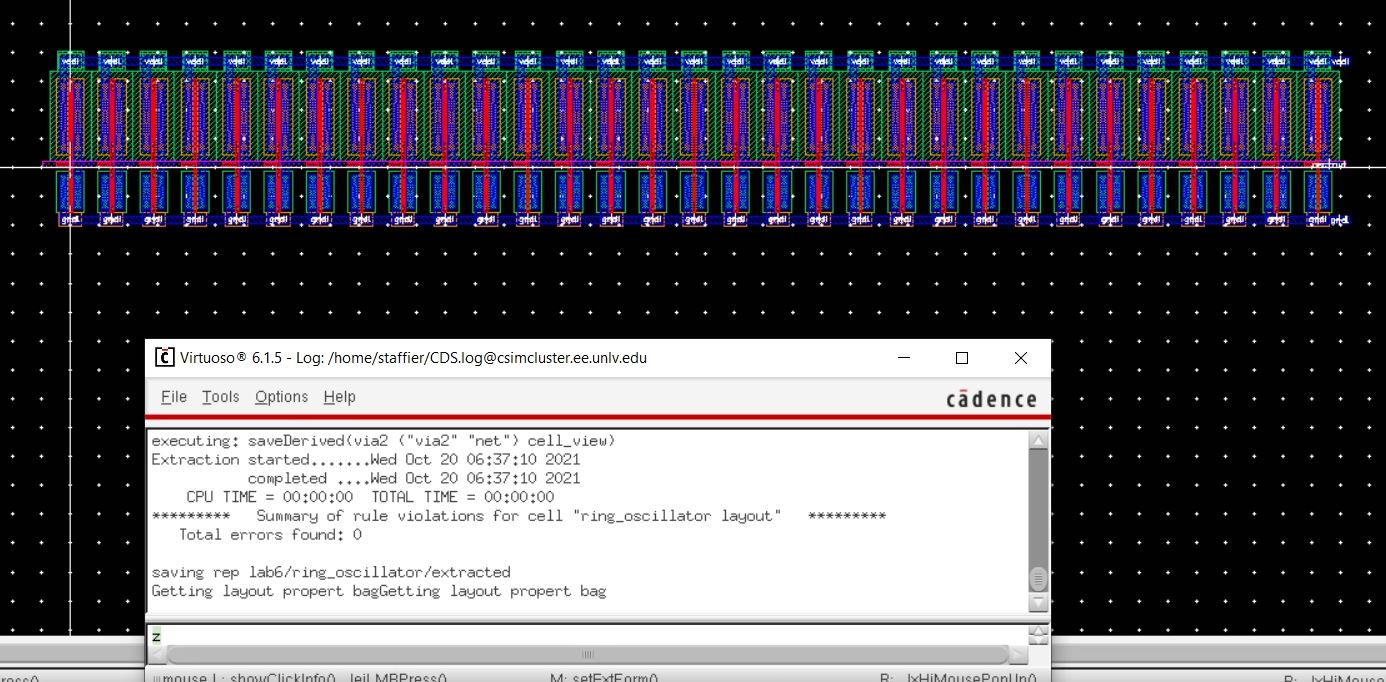
8-bit Full-Adder Extracted:

8-bit Full-Adder LVS Settings:

8-bit Full-Adder LVS Output:

Backup
My online backup of my completed files can be downloaded here.